
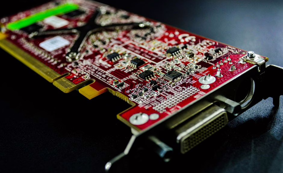
- AI models are built mostly from matrix multiplications, and GPUs dominate because they run thousands of those multiply-add operations in parallel.
- NVIDIA leads not only on silicon but on software: its CUDA platform is the de facto standard that most AI frameworks target.
- Google’s TPU is a custom ASIC built around a systolic array; AWS Trainium, Groq, and Cerebras are other specialised accelerators.
- Performance is increasingly bottlenecked by memory bandwidth, which is why High Bandwidth Memory (HBM) stacked next to the compute die is now decisive.
- Training and inference have different chip needs, and the whole supply chain — concentrated in a handful of firms and one foundry, TSMC — is now a geopolitical pressure point.
Why GPUs dominate AI
GPUs dominate AI because deep learning is dominated by matrix multiplication, and a GPU is a machine built to do many multiply-and-add operations at once. Where a CPU has a handful of powerful cores optimised for sequential tasks, a modern GPU has thousands of simpler cores that run the same operation across huge batches of numbers in parallel — exactly the workload a neural network needs.
The fit is no accident of marketing. Training a model means pushing data through layers of weighted sums — the linear algebra at the core of neural networks — and then back-propagating gradients, both of which reduce to dense matrix math. GPUs were designed to shade millions of pixels in parallel; that same parallelism turned out to be ideal for tensors. Around 2012 the AlexNet result, trained on a pair of NVIDIA GPUs, made the GPU-for-deep-learning pairing the industry default, and it has only deepened since.
From graphics to tensor cores
Modern data-centre GPUs are no longer general graphics parts. NVIDIA’s Tensor Cores, introduced with the Volta architecture in 2017, are dedicated units that perform small matrix multiplies in a single operation, often in reduced precision such as FP16, BF16, or FP8. Lower precision means more operations per second and less memory traffic, which is why mixed-precision training — performing most math in 16-bit and accumulating in higher precision — has become standard practice for large models.
NVIDIA and the CUDA moat
NVIDIA’s dominance rests as much on software as on hardware. Its CUDA programming platform, launched in 2007, lets developers write general-purpose code for the GPU, and over nearly two decades it has accumulated the libraries, tooling, and community that AI frameworks like PyTorch and TensorFlow are built on. Switching away from CUDA means rebuilding a large software stack, which gives NVIDIA a durable advantage often called its moat.
Why the moat is hard to cross
Competitors can match raw FLOPS, but matching CUDA’s mature kernels, debuggers, and framework integration is harder. AMD’s ROCm and Intel’s oneAPI are the main open challengers, and higher-level compilers such as OpenAI’s Triton aim to let developers write hardware-agnostic kernels. Progress is real but incremental; for most teams in 2026 the path of least resistance still runs through CUDA and NVIDIA silicon.
The economics
That lock-in shows up in NVIDIA’s results. The company’s data-centre revenue grew several-fold across 2023–2024 as demand for its H100 and successor parts outstripped supply, and individual accelerators have at times sold for tens of thousands of dollars apiece. The scarcity of top GPUs has itself become a strategic resource for the labs racing to train frontier models.
TPUs and custom accelerators
Beyond GPUs, several companies build custom accelerators — application-specific integrated circuits (ASICs) designed only for machine learning. The best known is Google’s Tensor Processing Unit, first deployed internally around 2015 and now in its later generations. Unlike a flexible GPU, a TPU is purpose-built for tensor math, which can make it more efficient for the workloads it targets.
How a TPU works
According to Google’s documentation, the TPU is built around a systolic array: a large grid of multiply-accumulate units wired directly to one another so that intermediate results flow between them without repeatedly touching memory. Google reports that early TPU generations used arrays on the order of 128×128 or 256×256 units, performing tens of thousands of multiply-adds per cycle while avoiding the memory traffic that limits more general designs. Reducing data movement is the whole point — moving numbers costs far more energy than computing on them.
The wider field
The accelerator landscape has widened well beyond Google. Amazon designs Trainium for training and Inferentia for inference inside AWS. Groq markets a deterministic “Language Processing Unit” aimed at very low-latency inference. Cerebras takes the opposite extreme with a wafer-scale engine — a single chip the size of a dinner plate carrying hundreds of thousands of cores. Each bets that specialising for the structure of transformers can beat a general GPU on cost or speed for some slice of the market.
Memory bandwidth and HBM
Memory bandwidth — how fast a chip can move data between memory and its compute units — has become the main bottleneck for large AI models, often more than raw arithmetic. A frontier model has tens or hundreds of billions of parameters that must be streamed to the compute units repeatedly, so a chip starved of bandwidth sits idle waiting for data, a condition engineers call being “memory-bound”.
What HBM changes
The answer is High Bandwidth Memory (HBM): DRAM dies stacked vertically and placed right next to the processor on the same package, connected by a very wide interface. The effect is dramatic. NVIDIA’s H100 with HBM3 reaches roughly 3.35 terabytes per second of memory bandwidth in its SXM form, per NVIDIA’s product materials — several times what conventional GDDR memory delivers. HBM supply, dominated by SK Hynix, Samsung, and Micron, has become as constrained as the GPUs themselves.
Why this dictates serving cost
Because generating each token requires reading the model’s weights from memory, inference speed and cost track memory bandwidth closely. Techniques like quantisation and batching exist largely to ease this pressure — a topic explored further in our guide to inference optimization. The practical upshot: when buyers compare AI chips, bandwidth and total memory capacity often matter more than headline FLOPS.
Training versus inference, and supply geopolitics
Training and inference stress chips differently, and the supply of both kinds of silicon has become a matter of national policy. Training a model is a massive one-time job favouring maximum throughput and huge clusters; inference — running the finished model for users — is a continuous, latency-sensitive workload where efficiency per query dominates. Many newer chips, such as Groq’s and AWS Inferentia, target inference specifically because that is where the long-run compute bill accumulates.
One foundry, many dependencies
Nearly all leading-edge AI chips — NVIDIA’s, Google’s, Amazon’s, AMD’s — are manufactured by a single Taiwanese foundry, TSMC, on advanced process nodes that only a few facilities worldwide can produce. The lithography machines that make those nodes come almost exclusively from the Dutch firm ASML. This concentration means a disruption at any one node ripples through the entire AI industry.
Export controls and strategy
Since 2022 the United States has restricted exports of the most advanced AI chips and chipmaking equipment to China, and has tightened those rules repeatedly since. The controls have reshaped product lines — vendors created throttled export variants — and accelerated efforts in several countries to build domestic capacity. Chip supply, once a back-office procurement detail, is now squarely a geopolitical lever over who can train frontier AI.
Frequently asked questions
Why are GPUs better than CPUs for AI?
GPUs are better for AI because deep learning is overwhelmingly matrix multiplication, and GPUs are built for massive parallelism — thousands of simpler cores doing the same multiply-add across large batches of data at once. A CPU has a few powerful cores tuned for sequential, branchy work and finishes these dense numeric workloads far more slowly. Modern data-centre GPUs also add dedicated Tensor Cores and very high memory bandwidth, widening the gap for neural-network training and inference specifically.
What is the difference between a GPU and a TPU?
A GPU is a relatively general parallel processor that handles graphics, scientific computing, and machine learning, programmed through ecosystems like CUDA. A TPU is an application-specific chip Google designed only for tensor math, built around a systolic array that streams data between compute units to minimise memory access. TPUs can be more efficient for the workloads they target but are far less flexible, and outside Google Cloud they are not generally available the way GPUs are.
Why does memory bandwidth matter so much for AI chips?
Large models have billions of parameters that must be repeatedly moved from memory to the compute units, so chips frequently sit idle waiting for data rather than running out of arithmetic — they are “memory-bound”. High Bandwidth Memory stacks DRAM beside the processor to move data far faster; NVIDIA’s H100 reaches roughly 3.35 TB/s. Because every generated token requires reading the weights, inference cost and speed track bandwidth closely, often making it more important than raw FLOPS.